ATtiny85 SPI protocol – Master and Slave mode tutorial
20 May 2025Serial communication protocols provides the means to communicate for microcontrollers with external hardware, peripherals or other microcontrollers. USART, SPI, I2C are some of the popular serial communication protocols in embedded world. In order to facilitate serial communication in ATtiny85 microcontroller it is equipped with a Universal Serial Interface USI module. This USI module can operate in Two wire Synchronous data transfer ( I2C protocol ) and Three wire Synchronous data transfer ( SPI protocol ) modes. This tutorial covers how to operate ATtiny85 in both SPI master and slave mode.
SPI protocol or Three wire Synchronous data transfer mode:
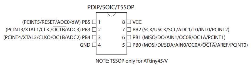
SPI is a form of serial communication that uses three pins to transfer data. In SPI communication the devices take the role of master and slave to establish communication. The master device is responsible for generating the clock pulse to synchronize the communication. Three mandatory pins of SPI communication in ATtiny85 are DO (PB1) , DI (PB0) and USCK (PB2). Additionally Slave Select ( SS ) pin can be configured in the code in case multiple slave devices are involved in the communication. Learn more about SPI communication in detail here.
Timing diagram of SPI protocol in ATtiny85:
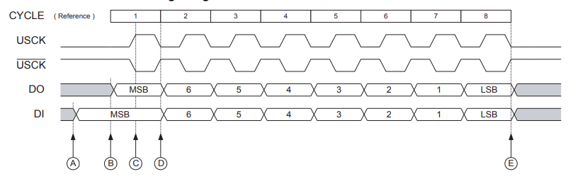
The above timing diagram briefs about SPI communication in ATtiny85. USCK is the clock cycle that synchronize the communication between devices. It can be external or internal ( generated by master device ). The data register associated with SPI communication is of 8 bit in length. DO shown above represents the data that goes out the sender device starting with MSB. DI shown above represents the data that comes in the receiver device starting with the MSB.
The point A and B at the above diagram represents that Data that need to be sent must be placed at the USIDR ( USI data register ) at least half a clock before USCK clock generation and the commencement of sampling. Also while receiving the data, MSB should be held in DI pin half a clock cycle before beginning of USCK sampling. This ensures sending of receiving of data bit in sync with the clock pulse. Each clock pulse will be sampled at rising and falling edges of the clock cycles. A 16 bit counter increments with each sampling ( rising and falling edges of clock pulse ).
The data bits 6, 5, 4,…. will be sent or received in sync with the trailing clock pulses. At the end of 8th clock pulse ( point E in above image ) all the 8 bits would have been sent or received and counter would have reached the maximum value. Upon reaching its maximum value Counter overflow flag raises indicating the data transfer is complete and now the next byte can be sent or received via data lines.
Slave select in ATtiny85: Slave select is the feature used in SPI when one master need to communicate with multiple slaves. For the purpose of slave select an individual pin must be assigned from the master device. If a master need to communicate with two slave devices two slave select pins must be assigned. When master device wish to send or receive data from slave-1 device, it will pull the slave select pin assigned to that slave-1 to low state. Now the slave-1 and master can communicate with each other.
In ATtiny85 there is no dedicated slave select pin. It need to be established by means of software meaning you to have use a IO pin and assign it as input if your device is a slave and when the input goes low, you need to activate the SPI communication. Whereas if your device is a master you have assign a IO pin as output and pull it to low to establish communication with a slave device.
USICR ( USI Control Register )
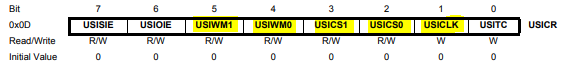
The bits USIWM1 and USIWM0 bits in the USICR register is used to set the USI module to operate using SPI protocol or I2C protocol. The below table shows the bit settings for choosing the SPI communication.
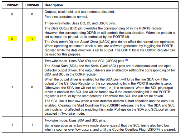
The bits USIWM1 and USIWM0 has to be set as 0 and 1 in order for our USI module to operate in SPI mode.
USICS0, USICS1 and USICLK bits are used to select the clock that will be used for SPI communication. The below table shows the various clock sources that can be used for our SPI communication and clock to power a 4 bit counter which is responsible for keeping the track of data sent or received ( explained below ).
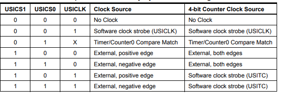
Possible clock sources are Software generated using the USICLK bit, external clock to USCK or PB2 pin and Timer/ Counter0 compare match. In this tutorial we are going to use Software generate clock strobe ( USICLK ).
When USICLK bit is written as 1, single clock transition will be generated internally to power SPI communication. This enables USIDR register to send or receive single bit of data. Therefore bit has to be written high 16 times to send or receive a byte of data.
USITC is a bit that is responsible for generating clock pulse in case if we are using our microcontroller as master to generate clock pulse. Writing of this bit toggles the logic state in USCK pin from 0 to 1 or 1 to 0. This provides a way to generate clock pulse and synchronize data transfer with slave devices.
USIDR ( USI Data register ):
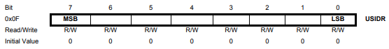
This the actual register which holds the data that need to be sent and the data that is received from other devices. User need to write 8 bit data in this register and then transmit the data by activating clock pulses to synchronize the transfer. Similarly when the ATtiny85 receives the data each bit received and placed in the USIDR register. When transfer of a byte is complete, data in USIDR register will be copied to USIBR register.
USIBR ( USI Buffer register ):
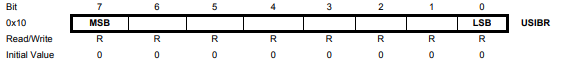
This is the similar to the USI data register. Contents of USIDR register will be copied to USI Buffer register when data transfer is complete. This provides user with time to read the data when the data transfer is time sensitive.
USISR ( USI status register ):
Status register is used to identify the status of USI peripheral. The bits USICNT0, USICNT1, USICNT2, USICNT3 are dedicated counter bits that keep count of the data transfer. It does that by incrementing by one every raising and falling edge of clock pulse. 4 bits are dedicated for this counter, therefore the count data will overflow after counting to 16, that is this counter will overflow after transfer of every byte.
In this register USIOIF bit is an overflow flag bit which will overflow when the above counter overflows after reaching 16 value. This flag will be read as one when a data byte transfer is completed.
Circuit diagram – ATtiny85 MCUs as Master and Slave:
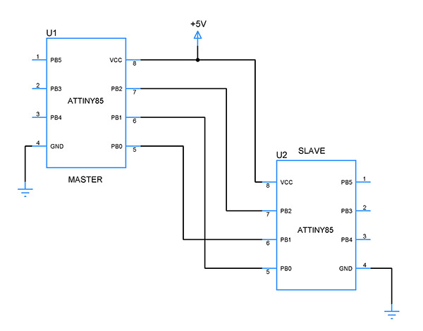
attiny85-spi-protocol-master-slave-deviceIn this setup U1 acts like Master and U2 will be the slave. U1 generates clock pulse to synchronize this SPI protocol communication.
Steps to configure ATtiny85 and send data as master using SPI protocol: Use the data direction register DDRB to set pins DO (PB0), DI (PB1) and USCK (PB2) as output, input and input. Using the bits USIWM1 and USIWM0 bit in USICR register select the three wire mode aka SPI Place the data byte that need to sent to slave in USIDR register Clock the data transmission using the bits USICS1, USICS0 and USICLK. In this tutorial we are going to use Software strobe as clock so the these three bits will be written as 001. Write the USITC bit high to toggle the USICLK pin which will serve as clock source to the slave. Repeat the steps 4 and 5 until the USIOIF flag is raised to complete one byte data transfer Write the next byte to USIDR register Repeat the steps 4 and 5. Sample Code for ATtiny85 as SPI master device:
#include<avr/io.h>
String tosend="Test";

void spi_setup()
{
  DDRB=(1<<PB1)|(1<<PB2);     //Setting direction of PB1 and PB2 as output
  USICR=(1<<USIWM0);          //Choosing SPI aka three wire mode
}

int main()
{
  short int i=0;
  spi_setup();
  for(i=0;i<=3;i++)
  {
   USIDR=tosend[i];          //Writing data bytes in Data register
   while(USIOIF==0)         //Checking USI data counter overflow flag to detect the end of transmission every byte
   {
    USICR|=(1<<USICLK)|(1<<USITC);  //Enabling clock for transmission and generating clock for slave device
   }
   USISR|=(1<<USIOIF);             //Clearing counter overflow flag
  }
}
ATtiny85 as SPI slave: To configure SPI as slave device it need to be configured to take external clock pulse using USICS0, USICS1 and USCLK bits to take input from the master device. The input clock pulse from master device must be fed to USCK pin or PB2. The direction of this pin must be set to input using DDRB register.
Steps to configure ATtiny85 to receive data as SPI slave: Use the data direction register DDRB to set pins DO (PB0), DI (PB1) and USCK (PB2) as output, input and input. Using the bits USIWM1 and USIWM0 bit in USICR register select the three wire mode aka SPI Choose the clock source as External positive edge and external both edges for 4 bit counter. Wait until the USIOIF flag goes high, this indicates one byte has been received. Copy the data from USIBR register for processing. Repeat from step 4. Sample Code for ATtiny85 as SPI slave device:
#include<avr/io.h>
String received[200];

void spi_setup()
{
  DDRB=(1<<PB1);     //Setting direction of PB1
  USICR=(1<<USIWM0);          //Choosing SPI aka three wire mode
}

int main()
{
  int i=0;
  spi_setup();
  while(1)
  {
   if((USISR&(1 << USIOIF))==1)         //Checking USI data counter overflow flag to detect the end of transmission every byte
   {
    received[i]=USIBR;  //Reading received byte from USIBR buffer register
    if(i<200)
     i=i+9;
    else
     i=0;
    USISR|=(1<<USIOIF);  //Clearing counter overflow flag
   }
  }
}
Try this out:
- et up two ATtiny85 with one being master and other being slave. Write code for both Master and Slave device with slave select functionality.
- Master device should send a string “Welcome” and Slave responding back “Ok” upon successfully receiving the data.